Auto-focus microscope, MEMS Metrology, automation
Auto-focus MEMS inspection microscope

XYZ Autofocus Metrology Microscopes

Full capability to design, manufacture and install microscope-based metrology and inspection system including material handling for MEMS and/or semiconductor applications

  • Infinity corrected objectives
  • On-axis top and bottom strobe LED lighting
  • In-tray inspection
  • 4M pixel, 160 FPS camera, 25M pixel, 84 FPS camera
  • High-speed processing
  • LED strobe lighting, collimating optics and controllers

Anamorphic objective, wafer scanner, micro- bumps
3D anamorphic wafer scanner objective

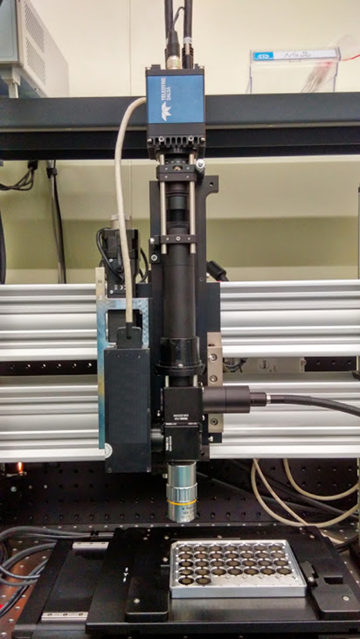
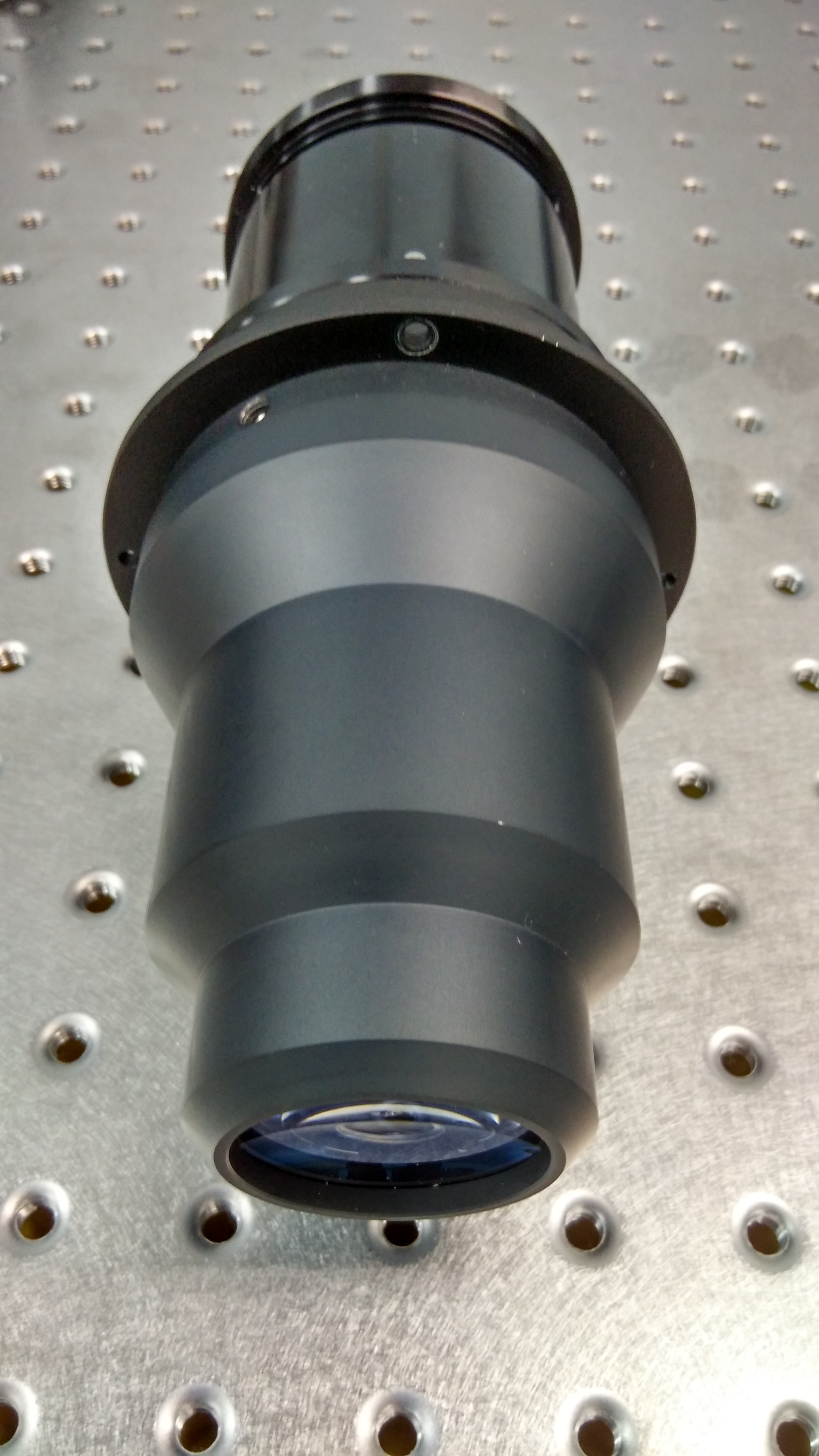
3D Anamorphic Imaging Lenses

Our family of 3D lenses has a wide range of inspection and metrology applications for semiconductors and electronics from BGA substrates to microbumps on silicon interposers. These lenses are tuned for laser triangulation applications and have higher magnification in vertical axis allowing much better height measuring performance, while keeping lower magnification in horizontal axis increasing field of view thus the speed.

objectives

3D camera lens, wafer scanner, microbumps
3D camera tube lens

Wafer scanner, Laser triangulation line projector

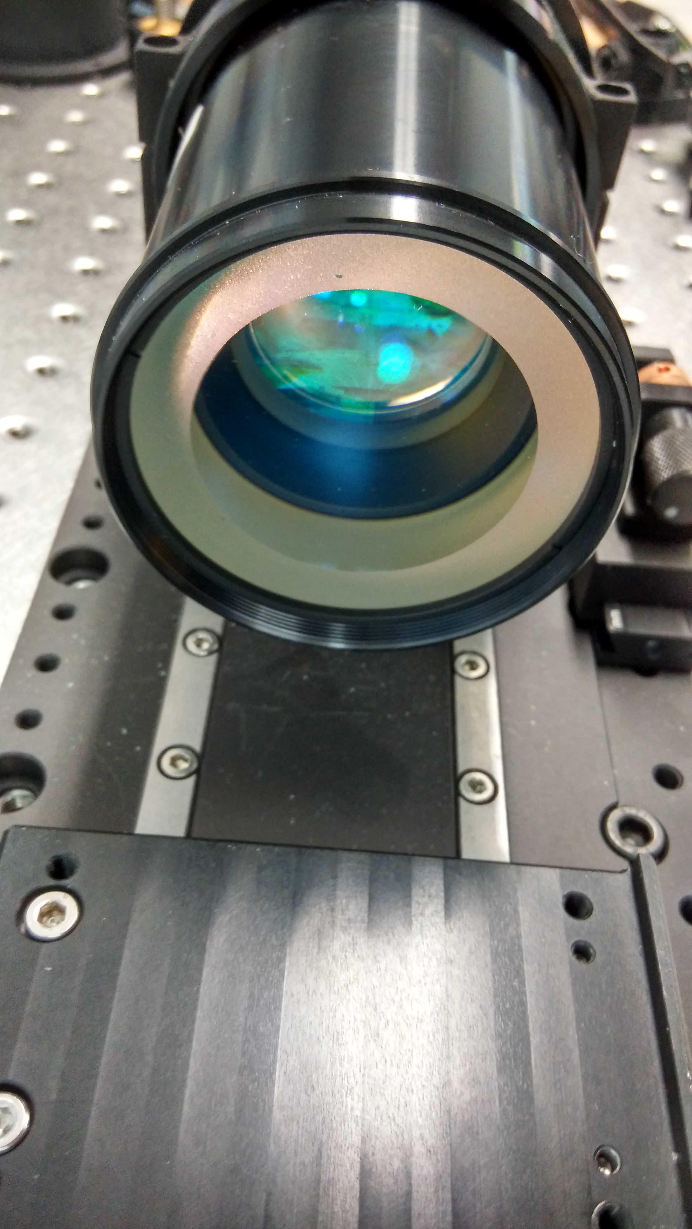
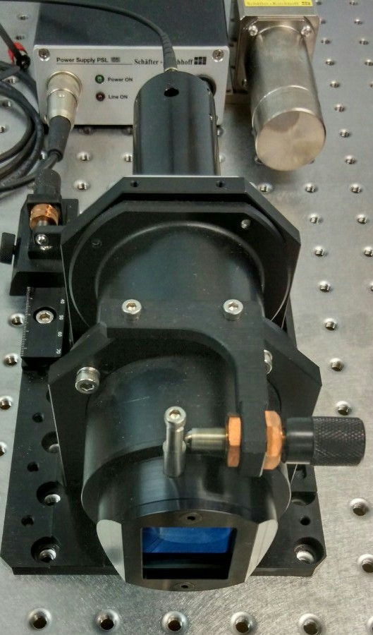
Lasers & Line Projections Optics

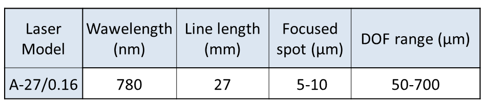
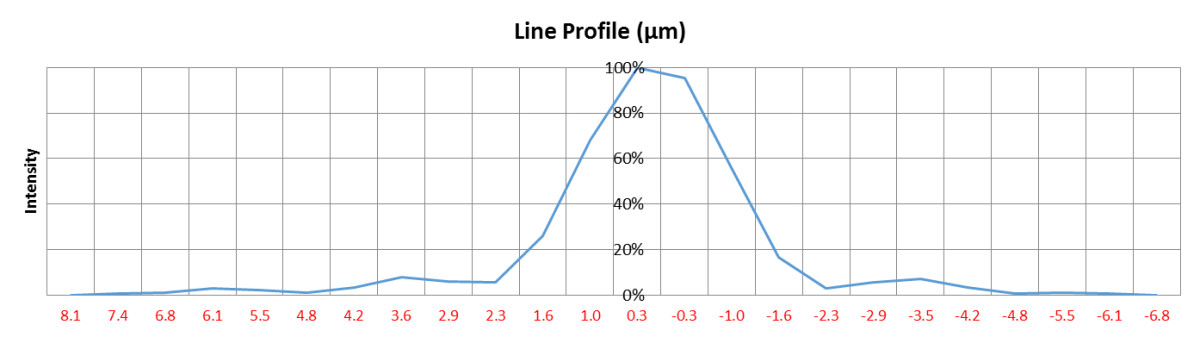
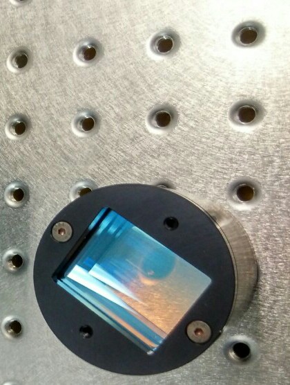
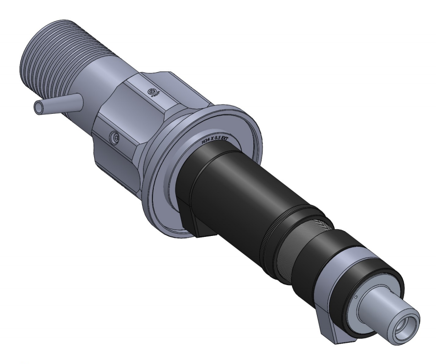
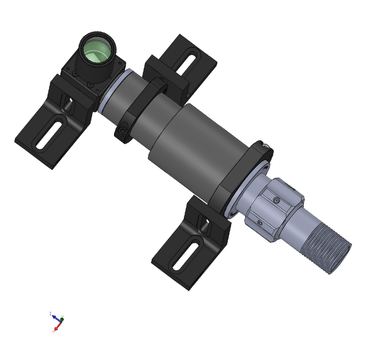
We typically integrate Schafter & Kirkhoff laser products with our custom collimators and high NA line projector lenses. Applications of these lenses are 3D laser triangulation for semiconductor and electronics applications. High resolution thin laser line is ideal for wafer μbumps scanning allowing sub-micron accuracy and repeatability.

laser spec

Thin laser line, laser triangulation, Wafer scanner


Laser line projector optics, wafer scanner
Laser line projector optics

Wafer bumps: Laser triangulation images and processing

3D camera, laser triangulation

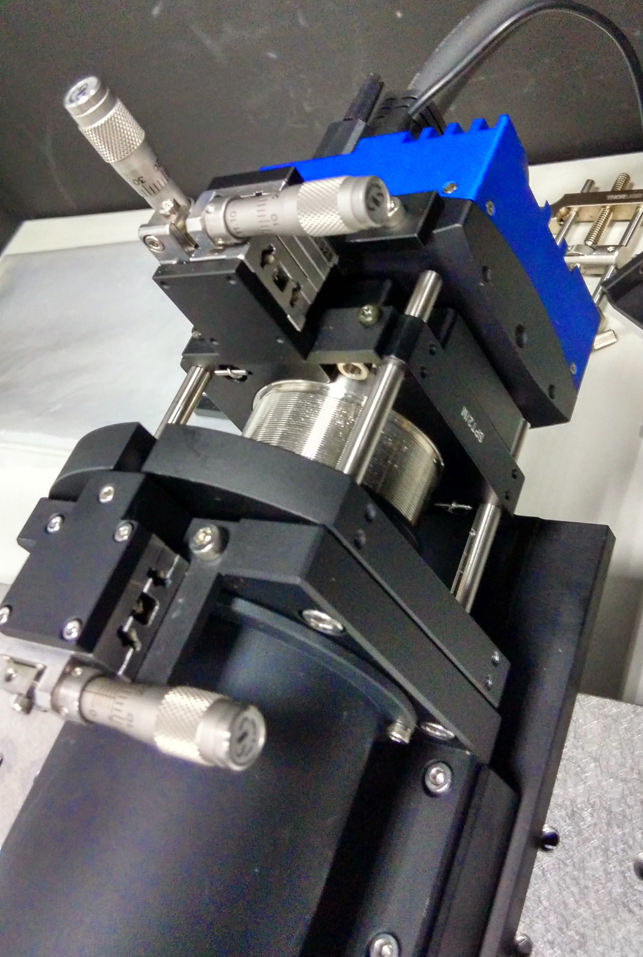
3D high speed camera capable of over 2.2G pixels per second


High Speed 3D Camera and Processing

Custom firmware 4M pixel camera could run at over 30,000 FPS and over 2.2GB data rates for typical laser triangulation applications for semiconductor industry. Individually programmable windows allow for independent exposures. Images are transferred via CoaxExpress link to PC memory. Acquired images are processed with subpixel precision in real time on GPU.  These sophisticated algorithms allow both high accuracy and repeatability of results. 

For high precision, high magnification application, camera - lens boresight can be adjusted as well as the camera alignment with scanning axes in object space within few pixels.

awesome-nvidia-wallpaper-3473-3687-hd-wallpapers


Lighting

Custom LED strobe lighting design