
Wafer μBumps 3D Scan
Services
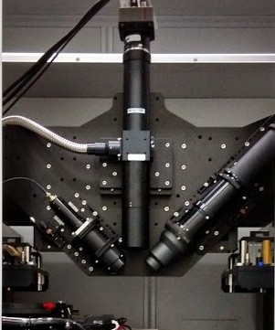
High performance 2D and 3D metrology and inspection for semiconductor industry: Wafer, CSP strips, MEMS, etc.
Design
- System design: wafer, CSP substrates, MEMS etc,
- Laser and camera optics,
- Mechanical: sensors and electro-optics, motion system
- Electrical / electronics: camera, laser, automation, vision processing, etc
- Software: vision algorithms and inspection systems.
Manufacturing
- Part procurement
- Assembly
- Testing
- Quality control
- Packing & Shipping
Installation
- Installation support at OEM and end user
- Commissioning support
Support
- Spare parts
- Warranty
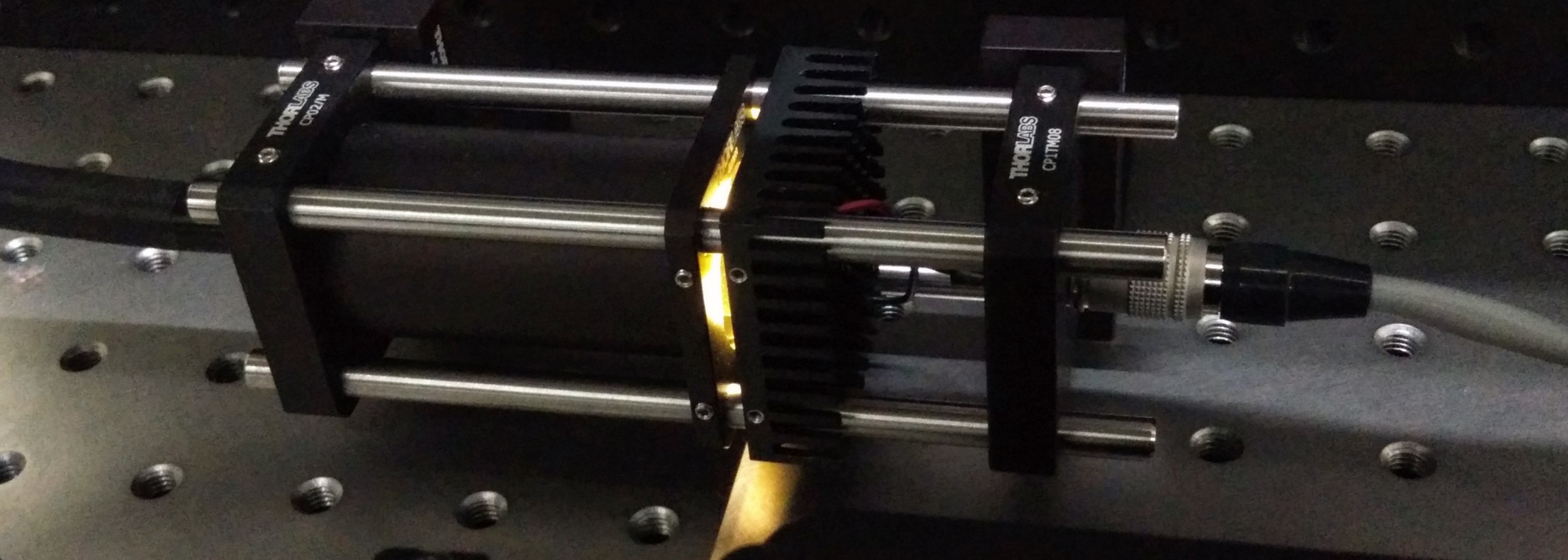
 Fiber optics coupled LED lamp